


द्रोण - 1 SUPER TET Offline Cum Online batch ORAI Branch
28 July, 2026


Enter your Email ID and we'll send you a link to get back into your account.

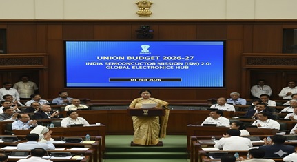

India Semiconductor Mission 2.0
Tue 03 Feb, 2026
Context:
Key Points:
India Semiconductor Mission 1.0
Major Schemes under ISM
Major Achievements
What is a Semiconductor?
Properties of Semiconductors
Types of Semiconductors
Uses of Semiconductors :
Semiconductors form the backbone of electronic devices and are used in:
28 July, 2026
27 July, 2026
22 July, 2026
20 July, 2026
26 May, 2026
08 May, 2026
20 April, 2026
01 April, 2026
01 April, 2026
16 March, 2026
